{var%20f='http://v.t.sina.com.cn/share/share.php?appkey=1515056452',u=z||d.location,p=['&url=',e(u),'&title=',e(t||d.title),'&source=',e(r),'&sourceUrl=',e(l),'&content=',c||'gb2312','&pic=',e(p||'')].join('');function%20a(){if(!window.open([f,p].join(''),'mb',['toolbar=0,status=0,resizable=1,width=440,height=430,left=',(s.width-440)/2,',top=',(s.height-430)/2].join('')))u.href=[f,p].join('');};if(/Firefox/.test(navigator.userAgent))setTimeout(a,0);else%20a();})(screen,document,encodeURIComponent,'','','https://www.xiaopingtou.cn/data/attach/logo/logo.png', '推荐 mljda 的问题《[文档]使用‘双向’leds实现十分低成本的传感器和通信【ledtouch同理】自译稿》','https://www.xiaopingtou.net/q-170387.html','页面编码gb2312|utf-8默认gb2312'));)
Very Low-Cost Sensing and Communication
Using Bidirectional LEDs
使用双向leds实现十分低成本的传感器和通信
[未完8/19][PIC单片机]
2 The Bidirectional LED Interface
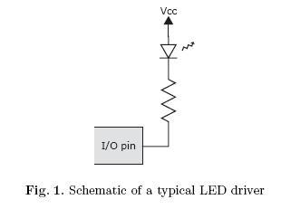
Light emitting diodes emit light in a fairly narrow frequency band when a small current is applied in the correct direction. Because the current-voltage characteristic is exponential, it is difficult to control a voltage applied directly across an LED accurately enough to attain a desired current; some means must be used to limit the current. In discrete systems, this is typically done by placing a resistor in series as shown in Figure 1. Since most microprocessor I/O pins can sink more current than they can source, the configuration shown in the figure is the most common way of driving an LED from a microprocessor.
双向LED接口
当一小电流被施加在一个正确的方向,发光二极管在一个狭窄的频道的释放光。因为电流-电压特性是指数性的,控制直接通过LED的准确足够的电压达到一个期望电流值是困难的;大多数方法必须限制电流。在独立系统,如图一展示的,串入一个电阻是典型的用法。在那以后,大多数单片机引脚能降低电流,途中展示的配置是大多数单片机驱动LED的普通用法。
The LED is a photodiode that is sensitive to light at and above the wavelength at which it emits (barring any filtering effects of a colored plastic package). Under reverse bias conditions, a simple model for the LED is a capacitor in parallel with a current source which models the optically induced photocurrent. (see Figure 2, [3]). It is this photocurrent that we would like to measure.
An inexpensive way to make a photodetector out of an LED is to tie the anode to ground and connect the cathode to a CMOS I/O pin driven high. This reverse biases the diode, and charges the capacitance. Next switch the I/O pin to input mode, which allows the photocurrent to discharge the capacitance down to the digital input threshold. By timing how long this takes, we get a measurement of the photocurrent and thus the amount of incident light. This sequence is shown in Figure 3.
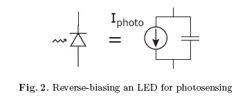
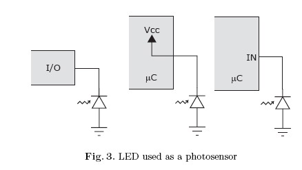
这LED是 对它发出的波长光敏感的光电二极管(除了任何有 {MOD}塑料封装引起的过滤器效应。)在反向偏置情况,LED的一个简单的模型 是一个电容并接一个光学反应产生电流的电流源,见图2,3。它是光电流如同我们喜欢测量的那样。一个便宜的方法来实现光检测器,连接阳极到地并连接阴极到一个高电平驱动的CMOS I/O引脚。这是反响偏置的二极管,且给电容充电。下一步选择这I/O引脚到输入模式,其允许光电流释放电容电压降至数字逻辑输入阀值,同时记时过程使用时间,我们能得到一个入射光电流总量的测量值,顺序在图3.
The circuits of Figures 1 and 2 can be combined to create a general bidirectional microprocessor interface to an LED as shown in Figure 4. This is identical to the circuit of Figure 1, except that now the resistor/LED combination is placed between two I/O pins.
Figure 5 shows how the pins are driven for the two modes. Figure 5a shows the “Emitting” mode where current is driven in the forward direction, lighting the LED. Figure 5b shows “Reverse Bias” mode, which charges the capacitance and prepares the system for measurement. The actual measurement is made in “Discharge” mode shown in Figure 5c. Since the current flowing into a CMOS input is extremely small, the low value current limiting resistor has little impact on the voltage seen at the input pin. As before, we simply time how long it takes for the photocurrent to discharge the capacitance to the pin’s digital input threshold. The result is a simple circuit that can switch between emitting and receiving light.
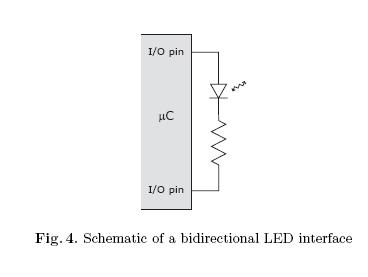
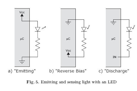
图1,2的电路能被者整合成一个如图4的通用双向单片机接口至led。这是完全相同的电路如图1,除了连接在两个引脚间的电阻/LED。
图5展示了怎么驱动引脚在两个模式,图5a展示在正向电流驱动下的”发光模式”,点亮LED。图5b展示了”反向偏置”模式,给电容充电并准备测量系统。 图5c展示 真正的测量作用于“释放”模式。
当电流流入一个CMOS输入时极小时,低值的限流电阻作用在输入引脚电压上的影响(冲击)低。在之前,我们简单的计量了光电流释放电容(电压)到引脚数字输入阀值。这个结果是一个在发射和接受光线间的简单电流值。
Because the circuit changes required to provide this bidirectional communication feature consist of only one additional I/O pin and printed circuit board trace (which can be provided at design time for zero additional hardware cost) we claim that adding this hardware feature to a device is essentially free. Of course, software and CPU runtime are also necessary to make this work.
Compare this to the cost of adding IrDA [7] (about $7) or Bluetooth [8] (more than $10) to a product. Using even a simple mechanical connector can cost several dollars because of the required level-shifting and electrostatic discharge (ESD) protection circuitry. Using an existing LED for communication can also save manufacturing costs because expensive plastic molds for the housing need not be altered to accommodate a dedicated infrared transceiver, antenna or physical connector.

-----全原文--------------
点击此处打开ourdev_185962.pdf(文件大小:531K)
Using Bidirectional LEDs
使用双向leds实现十分低成本的传感器和通信
[未完8/19][PIC单片机]
2 The Bidirectional LED Interface
Light emitting diodes emit light in a fairly narrow frequency band when a small current is applied in the correct direction. Because the current-voltage characteristic is exponential, it is difficult to control a voltage applied directly across an LED accurately enough to attain a desired current; some means must be used to limit the current. In discrete systems, this is typically done by placing a resistor in series as shown in Figure 1. Since most microprocessor I/O pins can sink more current than they can source, the configuration shown in the figure is the most common way of driving an LED from a microprocessor.
双向LED接口
当一小电流被施加在一个正确的方向,发光二极管在一个狭窄的频道的释放光。因为电流-电压特性是指数性的,控制直接通过LED的准确足够的电压达到一个期望电流值是困难的;大多数方法必须限制电流。在独立系统,如图一展示的,串入一个电阻是典型的用法。在那以后,大多数单片机引脚能降低电流,途中展示的配置是大多数单片机驱动LED的普通用法。
The LED is a photodiode that is sensitive to light at and above the wavelength at which it emits (barring any filtering effects of a colored plastic package). Under reverse bias conditions, a simple model for the LED is a capacitor in parallel with a current source which models the optically induced photocurrent. (see Figure 2, [3]). It is this photocurrent that we would like to measure.
An inexpensive way to make a photodetector out of an LED is to tie the anode to ground and connect the cathode to a CMOS I/O pin driven high. This reverse biases the diode, and charges the capacitance. Next switch the I/O pin to input mode, which allows the photocurrent to discharge the capacitance down to the digital input threshold. By timing how long this takes, we get a measurement of the photocurrent and thus the amount of incident light. This sequence is shown in Figure 3.
这LED是 对它发出的波长光敏感的光电二极管(除了任何有 {MOD}塑料封装引起的过滤器效应。)在反向偏置情况,LED的一个简单的模型 是一个电容并接一个光学反应产生电流的电流源,见图2,3。它是光电流如同我们喜欢测量的那样。一个便宜的方法来实现光检测器,连接阳极到地并连接阴极到一个高电平驱动的CMOS I/O引脚。这是反响偏置的二极管,且给电容充电。下一步选择这I/O引脚到输入模式,其允许光电流释放电容电压降至数字逻辑输入阀值,同时记时过程使用时间,我们能得到一个入射光电流总量的测量值,顺序在图3.
The circuits of Figures 1 and 2 can be combined to create a general bidirectional microprocessor interface to an LED as shown in Figure 4. This is identical to the circuit of Figure 1, except that now the resistor/LED combination is placed between two I/O pins.
Figure 5 shows how the pins are driven for the two modes. Figure 5a shows the “Emitting” mode where current is driven in the forward direction, lighting the LED. Figure 5b shows “Reverse Bias” mode, which charges the capacitance and prepares the system for measurement. The actual measurement is made in “Discharge” mode shown in Figure 5c. Since the current flowing into a CMOS input is extremely small, the low value current limiting resistor has little impact on the voltage seen at the input pin. As before, we simply time how long it takes for the photocurrent to discharge the capacitance to the pin’s digital input threshold. The result is a simple circuit that can switch between emitting and receiving light.
图1,2的电路能被者整合成一个如图4的通用双向单片机接口至led。这是完全相同的电路如图1,除了连接在两个引脚间的电阻/LED。
图5展示了怎么驱动引脚在两个模式,图5a展示在正向电流驱动下的”发光模式”,点亮LED。图5b展示了”反向偏置”模式,给电容充电并准备测量系统。 图5c展示 真正的测量作用于“释放”模式。
当电流流入一个CMOS输入时极小时,低值的限流电阻作用在输入引脚电压上的影响(冲击)低。在之前,我们简单的计量了光电流释放电容(电压)到引脚数字输入阀值。这个结果是一个在发射和接受光线间的简单电流值。
Because the circuit changes required to provide this bidirectional communication feature consist of only one additional I/O pin and printed circuit board trace (which can be provided at design time for zero additional hardware cost) we claim that adding this hardware feature to a device is essentially free. Of course, software and CPU runtime are also necessary to make this work.
Compare this to the cost of adding IrDA [7] (about $7) or Bluetooth [8] (more than $10) to a product. Using even a simple mechanical connector can cost several dollars because of the required level-shifting and electrostatic discharge (ESD) protection circuitry. Using an existing LED for communication can also save manufacturing costs because expensive plastic molds for the housing need not be altered to accommodate a dedicated infrared transceiver, antenna or physical connector.
-----全原文--------------
点击此处打开ourdev_185962.pdf(文件大小:531K)
友情提示: 此问题已得到解决,问题已经关闭,关闭后问题禁止继续编辑,回答。
一周热门 更多>