{var%20f='http://v.t.sina.com.cn/share/share.php?appkey=1515056452',u=z||d.location,p=['&url=',e(u),'&title=',e(t||d.title),'&source=',e(r),'&sourceUrl=',e(l),'&content=',c||'gb2312','&pic=',e(p||'')].join('');function%20a(){if(!window.open([f,p].join(''),'mb',['toolbar=0,status=0,resizable=1,width=440,height=430,left=',(s.width-440)/2,',top=',(s.height-430)/2].join('')))u.href=[f,p].join('');};if(/Firefox/.test(navigator.userAgent))setTimeout(a,0);else%20a();})(screen,document,encodeURIComponent,'','','https://www.xiaopingtou.cn//data/attach/topic/topicKPo7gB.jpg', '推荐 topskycn123 的文章《DSP学习笔记(1)——F28335基础知识》','https://www.xiaopingtou.net/article-76951.html','页面编码gb2312|utf-8默认gb2312'));)
❤ 2019.3.6
今天开始学习DSP,over。
我用的版本是德州仪器的TMS320F28335,用的开发板是研旭的TMS320F28335至尊开发板,到底有多至尊我也不知道,不过看起来教材和资料挺全的。


 〇 基础知识
● DSP的历史
略(自己看书百度去)
● 数字信号处理特点
〇 基础知识
● DSP的历史
略(自己看书百度去)
● 数字信号处理特点
 ● DSP主要特点
 ● TI的芯片系列
 F28335系列属于C2000系列,在TI看来不属于DSP,属于MCU,但是我们就当成DSP学(?)
● C2000系列简介
F28335系列属于C2000系列,在TI看来不属于DSP,属于MCU,但是我们就当成DSP学(?)
● C2000系列简介
 ● DSP系统开发
 ● 如何成为一个优秀的DSP工程师
 (真的假的?)
● 教程总纲
(真的假的?)
● 教程总纲
 〇 DSP开发环境介绍
● CCS介绍
〇 DSP开发环境介绍
● CCS介绍
 ● CCS安装
(略)
● 仿真器
○ CCS6如何连接仿真器(这个手册上面有)
1、建立target configuration file
● CCS安装
(略)
● 仿真器
○ CCS6如何连接仿真器(这个手册上面有)
1、建立target configuration file
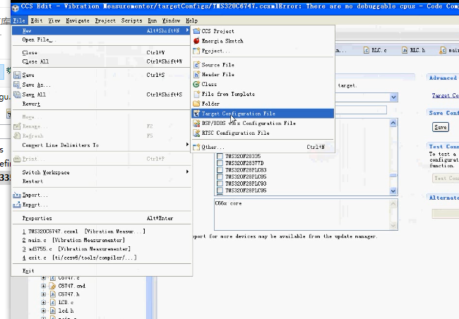 2、输入名字
 3、选择仿真器、芯片,然后点save
 ♣ 经常会在工程文件里生成一个target configuration 文件
 ❤ 2019.3.22
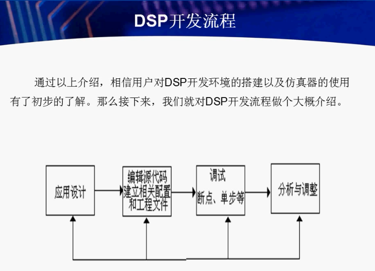
〇 DSP开发流程
❤ 2019.3.22
〇 DSP开发流程
 ○ CMD文件(配置文件)
指定DSP内部的硬件存储器的一些相关地址以及长度。
包含两部分:MEMORY以及SECTIONS
MEMORY:指定DSP内部的ram和flash的首地址以及长度
SECTIONS:指定程序组成部分对应内存的储存部分(MEMORY中设定的部分)。
〇 TMS320F28335介绍
○ CMD文件(配置文件)
指定DSP内部的硬件存储器的一些相关地址以及长度。
包含两部分:MEMORY以及SECTIONS
MEMORY:指定DSP内部的ram和flash的首地址以及长度
SECTIONS:指定程序组成部分对应内存的储存部分(MEMORY中设定的部分)。
〇 TMS320F28335介绍


 〇 时钟与看门狗
 ● 内部时钟


 ❤ 2019.3.23
● 外设时钟
❤ 2019.3.23
● 外设时钟

 ● 看门狗
● 看门狗


 ● 时钟及看门狗寄存器(英文版System Control and Interrupts Reference Guide P34)(中文版见《手把手》P83)
 ♣ System Control and Interrupts Reference Guide:官方下载地址
● 关于看门狗及时钟的初始化例子
打开官方例程的时钟配置文件
♣ System Control and Interrupts Reference Guide:官方下载地址
● 关于看门狗及时钟的初始化例子
打开官方例程的时钟配置文件
 观察系统时钟初始化函数


 如果需要启用watchdog,则用这个函数:
 可以知道需要启用watchdog的话需要先后写入这两个值。
○ 下面是锁相环初始化
可以知道需要启用watchdog的话需要先后写入这两个值。
○ 下面是锁相环初始化
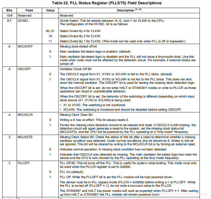
 首先看一下两个参数
 这个流程图配合寄存器说明来看


 稍微有点混乱,不过不需要看明白,反正用默认的就行,也就是10倍频,2分频,配合30M晶振,最后得到系统频率150M。
○ 初始化外设时钟
稍微有点混乱,不过不需要看明白,反正用默认的就行,也就是10倍频,2分频,配合30M晶振,最后得到系统频率150M。
○ 初始化外设时钟
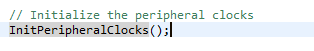 函数代码:
函数代码:
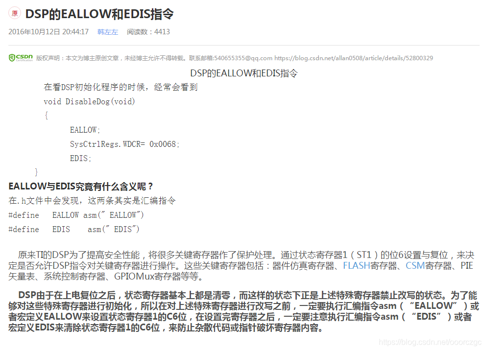 原文地址:DSP的EALLOW和EDIS指令
先看这段:
原文地址:DSP的EALLOW和EDIS指令
先看这段:
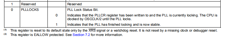
 我们先找到对应的寄存器说明:
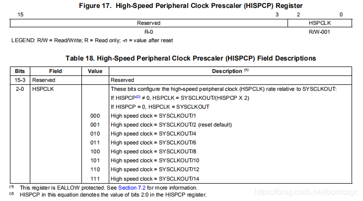
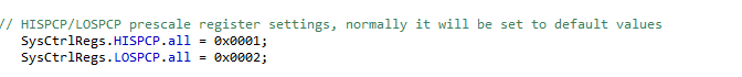
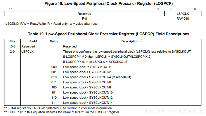 由上可知,这两句的意思是将高速时钟配置为2分频,将低速时钟配置为4分频。
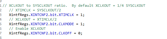 这个是用来控制时钟输出的,可以将时钟供给其他模块,可以省一个晶振(?)
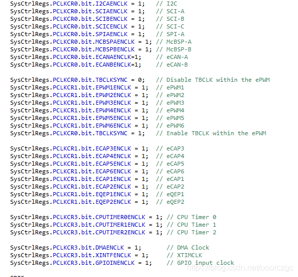
这个是用来控制外设时钟的开关,需要哪个模块就开哪个时钟,不用就关上,可以省电。
这个是用来控制时钟输出的,可以将时钟供给其他模块,可以省一个晶振(?)
这个是用来控制外设时钟的开关,需要哪个模块就开哪个时钟,不用就关上,可以省电。
〇 基础知识
● DSP的历史
略(自己看书百度去)
● 数字信号处理特点
● DSP主要特点
● TI的芯片系列
F28335系列属于C2000系列,在TI看来不属于DSP,属于MCU,但是我们就当成DSP学(?)
● C2000系列简介
● DSP系统开发
● 如何成为一个优秀的DSP工程师
(真的假的?)
● 教程总纲
〇 DSP开发环境介绍
● CCS介绍
● CCS安装
(略)
● 仿真器
○ CCS6如何连接仿真器(这个手册上面有)
1、建立target configuration file
2、输入名字
3、选择仿真器、芯片,然后点save
♣ 经常会在工程文件里生成一个target configuration 文件
❤ 2019.3.22
〇 DSP开发流程
○ CMD文件(配置文件)
指定DSP内部的硬件存储器的一些相关地址以及长度。
包含两部分:MEMORY以及SECTIONS
MEMORY:指定DSP内部的ram和flash的首地址以及长度
SECTIONS:指定程序组成部分对应内存的储存部分(MEMORY中设定的部分)。
〇 TMS320F28335介绍
〇 时钟与看门狗
● 内部时钟
❤ 2019.3.23
● 外设时钟
● 看门狗
● 时钟及看门狗寄存器(英文版System Control and Interrupts Reference Guide P34)(中文版见《手把手》P83)
♣ System Control and Interrupts Reference Guide:官方下载地址
● 关于看门狗及时钟的初始化例子
打开官方例程的时钟配置文件
//---------------------------------------------------------------------------
// InitSysCtrl:
//---------------------------------------------------------------------------
// This function initializes the System Control registers to a known state.
// - Disables the watchdog
// - Set the PLLCR for proper SYSCLKOUT frequency
// - Set the pre-scaler for the high and low frequency peripheral clocks
// - Enable the clocks to the peripherals

void InitSysCtrl(void)
{

   // Disable the watchdog
   DisableDog();

   // Initialize the PLL control: PLLCR and DIVSEL
   // DSP28_PLLCR and DSP28_DIVSEL are defined in DSP2833x_Examples.h
   InitPll(DSP28_PLLCR,DSP28_DIVSEL);

   // Initialize the peripheral clocks
   InitPeripheralClocks();
}
○ 第一个
//---------------------------------------------------------------------------
// Example: DisableDog:
//---------------------------------------------------------------------------
// This function disables the watchdog timer.

void DisableDog(void)
{
    EALLOW;
    SysCtrlRegs.WDCR= 0x0068;
    EDIS;
}
可以看到0x0068,转换成二进制就是0000 0000 0110 1000,查看watchdog的寄存器说明(英文版System Control and Interrupts Reference Guide P54)(中文版见《手把手》P88),可以知道其意义。
如果需要启用watchdog,则用这个函数:
//---------------------------------------------------------------------------
// Example: ServiceDog:
//---------------------------------------------------------------------------
// This function resets the watchdog timer.
// Enable this function for using ServiceDog in the application

void ServiceDog(void)
{
    EALLOW;
    SysCtrlRegs.WDKEY = 0x0055;
    SysCtrlRegs.WDKEY = 0x00AA;
    EDIS;
}
查看相应寄存器:
可以知道需要启用watchdog的话需要先后写入这两个值。
○ 下面是锁相环初始化
首先看一下两个参数
/*-----------------------------------------------------------------------------
      Specify the PLL control register (PLLCR) and divide select (DIVSEL) value.
-----------------------------------------------------------------------------*/
//#define DSP28_DIVSEL   0   // Enable /4 for SYSCLKOUT
//#define DSP28_DIVSEL   1 // Disable /4 for SYSCKOUT
#define DSP28_DIVSEL     2 // Enable /2 for SYSCLKOUT
//#define DSP28_DIVSEL     3 // Enable /1 for SYSCLKOUT

#define DSP28_PLLCR   10
//#define DSP28_PLLCR    9
//#define DSP28_PLLCR    8
//#define DSP28_PLLCR    7
//#define DSP28_PLLCR    6
//#define DSP28_PLLCR    5
//#define DSP28_PLLCR    4
//#define DSP28_PLLCR    3
//#define DSP28_PLLCR    2
//#define DSP28_PLLCR    1
//#define DSP28_PLLCR    0  // PLL is bypassed in this mode
//----------------------------------------------------------------------------
可以看出DSP28_PLLCR是倍频,DSP28_DIVSEL是分频,然后在看一下倍频与分频设置函数:
//---------------------------------------------------------------------------
// Example: InitPll:
//---------------------------------------------------------------------------
// This function initializes the PLLCR register.

void InitPll(Uint16 val, Uint16 divsel)
{

   // Make sure the PLL is not running in limp mode
   if (SysCtrlRegs.PLLSTS.bit.MCLKSTS != 0)
   {
      // Missing external clock has been detected
      // Replace this line with a call to an appropriate
      // SystemShutdown(); function.
      asm("        ESTOP0");
   }

   // DIVSEL MUST be 0 before PLLCR can be changed from
   // 0x0000. It is set to 0 by an external reset XRSn
   // This puts us in 1/4
   if (SysCtrlRegs.PLLSTS.bit.DIVSEL != 0)
   {
       EALLOW;
       SysCtrlRegs.PLLSTS.bit.DIVSEL = 0;
       EDIS;
   }

   // Change the PLLCR
   if (SysCtrlRegs.PLLCR.bit.DIV != val)
   {

      EALLOW;
      // Before setting PLLCR turn off missing clock detect logic
      SysCtrlRegs.PLLSTS.bit.MCLKOFF = 1;
      SysCtrlRegs.PLLCR.bit.DIV = val;
      EDIS;

      // Optional: Wait for PLL to lock.
      // During this time the CPU will switch to OSCCLK/2 until
      // the PLL is stable.  Once the PLL is stable the CPU will
      // switch to the new PLL value.
      //
      // This time-to-lock is monitored by a PLL lock counter.
      //
      // Code is not required to sit and wait for the PLL to lock.
      // However, if the code does anything that is timing critical,
      // and requires the correct clock be locked, then it is best to
      // wait until this switching has completed.

      // Wait for the PLL lock bit to be set.

      // The watchdog should be disabled before this loop, or fed within
      // the loop via ServiceDog().

	  // Uncomment to disable the watchdog
      DisableDog();

      while(SysCtrlRegs.PLLSTS.bit.PLLLOCKS != 1)
      {
	      // Uncomment to service the watchdog
          // ServiceDog();
      }

      EALLOW;
      SysCtrlRegs.PLLSTS.bit.MCLKOFF = 0;
      EDIS;
    }

    // If switching to 1/2
	if((divsel == 1)||(divsel == 2))
	{
		EALLOW;
	    SysCtrlRegs.PLLSTS.bit.DIVSEL = divsel;
	    EDIS;
	}

	// If switching to 1/1
	// * First go to 1/2 and let the power settle
	//   The time required will depend on the system, this is only an example
	// * Then switch to 1/1
	if(divsel == 3)
	{
		EALLOW;
	    SysCtrlRegs.PLLSTS.bit.DIVSEL = 2;
	    DELAY_US(50L);
	    SysCtrlRegs.PLLSTS.bit.DIVSEL = 3;
	    EDIS;
    }
}
有点乱,看不懂,但是ti贴心的(真的么?)画了个流程图:
这个流程图配合寄存器说明来看
稍微有点混乱,不过不需要看明白,反正用默认的就行,也就是10倍频,2分频,配合30M晶振,最后得到系统频率150M。
○ 初始化外设时钟
函数代码:
//--------------------------------------------------------------------------
// Example: InitPeripheralClocks:
//---------------------------------------------------------------------------
// This function initializes the clocks to the peripheral modules.
// First the high and low clock prescalers are set
// Second the clocks are enabled to each peripheral.
// To reduce power, leave clocks to unused peripherals disabled
//
// Note: If a peripherals clock is not enabled then you cannot
// read or write to the registers for that peripheral

void InitPeripheralClocks(void)
{
   EALLOW;

// HISPCP/LOSPCP prescale register settings, normally it will be set to default values
   SysCtrlRegs.HISPCP.all = 0x0001;
   SysCtrlRegs.LOSPCP.all = 0x0002;

// XCLKOUT to SYSCLKOUT ratio.  By default XCLKOUT = 1/4 SYSCLKOUT
   // XTIMCLK = SYSCLKOUT/2
   XintfRegs.XINTCNF2.bit.XTIMCLK = 1;
   // XCLKOUT = XTIMCLK/2
   XintfRegs.XINTCNF2.bit.CLKMODE = 1;
   // Enable XCLKOUT
   XintfRegs.XINTCNF2.bit.CLKOFF = 0;

// Peripheral clock enables set for the selected peripherals.
// If you are not using a peripheral leave the clock off
// to save on power.
//
// Note: not all peripherals are available on all 2833x derivates.
// Refer to the datasheet for your particular device.
//
// This function is not written to be an example of efficient code.

   SysCtrlRegs.PCLKCR0.bit.ADCENCLK = 1;    // ADC

   // *IMPORTANT*
   // The ADC_cal function, which  copies the ADC calibration values from TI reserved
   // OTP into the ADCREFSEL and ADCOFFTRIM registers, occurs automatically in the
   // Boot ROM. If the boot ROM code is bypassed during the debug process, the
   // following function MUST be called for the ADC to function according
   // to specification. The clocks to the ADC MUST be enabled before calling this
   // function.
   // See the device data manual and/or the ADC Reference
   // Manual for more information.

   ADC_cal();


   SysCtrlRegs.PCLKCR0.bit.I2CAENCLK = 1;   // I2C
   SysCtrlRegs.PCLKCR0.bit.SCIAENCLK = 1;   // SCI-A
   SysCtrlRegs.PCLKCR0.bit.SCIBENCLK = 1;   // SCI-B
   SysCtrlRegs.PCLKCR0.bit.SCICENCLK = 1;   // SCI-C
   SysCtrlRegs.PCLKCR0.bit.SPIAENCLK = 1;   // SPI-A
   SysCtrlRegs.PCLKCR0.bit.MCBSPAENCLK = 1; // McBSP-A
   SysCtrlRegs.PCLKCR0.bit.MCBSPBENCLK = 1; // McBSP-B
   SysCtrlRegs.PCLKCR0.bit.ECANAENCLK=1;    // eCAN-A
   SysCtrlRegs.PCLKCR0.bit.ECANBENCLK=1;    // eCAN-B

   SysCtrlRegs.PCLKCR0.bit.TBCLKSYNC = 0;   // Disable TBCLK within the ePWM
   SysCtrlRegs.PCLKCR1.bit.EPWM1ENCLK = 1;  // ePWM1
   SysCtrlRegs.PCLKCR1.bit.EPWM2ENCLK = 1;  // ePWM2
   SysCtrlRegs.PCLKCR1.bit.EPWM3ENCLK = 1;  // ePWM3
   SysCtrlRegs.PCLKCR1.bit.EPWM4ENCLK = 1;  // ePWM4
   SysCtrlRegs.PCLKCR1.bit.EPWM5ENCLK = 1;  // ePWM5
   SysCtrlRegs.PCLKCR1.bit.EPWM6ENCLK = 1;  // ePWM6
   SysCtrlRegs.PCLKCR0.bit.TBCLKSYNC = 1;   // Enable TBCLK within the ePWM

   SysCtrlRegs.PCLKCR1.bit.ECAP3ENCLK = 1;  // eCAP3
   SysCtrlRegs.PCLKCR1.bit.ECAP4ENCLK = 1;  // eCAP4
   SysCtrlRegs.PCLKCR1.bit.ECAP5ENCLK = 1;  // eCAP5
   SysCtrlRegs.PCLKCR1.bit.ECAP6ENCLK = 1;  // eCAP6
   SysCtrlRegs.PCLKCR1.bit.ECAP1ENCLK = 1;  // eCAP1
   SysCtrlRegs.PCLKCR1.bit.ECAP2ENCLK = 1;  // eCAP2
   SysCtrlRegs.PCLKCR1.bit.EQEP1ENCLK = 1;  // eQEP1
   SysCtrlRegs.PCLKCR1.bit.EQEP2ENCLK = 1;  // eQEP2

   SysCtrlRegs.PCLKCR3.bit.CPUTIMER0ENCLK = 1; // CPU Timer 0
   SysCtrlRegs.PCLKCR3.bit.CPUTIMER1ENCLK = 1; // CPU Timer 1
   SysCtrlRegs.PCLKCR3.bit.CPUTIMER2ENCLK = 1; // CPU Timer 2

   SysCtrlRegs.PCLKCR3.bit.DMAENCLK = 1;       // DMA Clock
   SysCtrlRegs.PCLKCR3.bit.XINTFENCLK = 1;     // XTIMCLK
   SysCtrlRegs.PCLKCR3.bit.GPIOINENCLK = 1;    // GPIO input clock

   EDIS;
}
♣ 首先注意的是EALLOW和EDIS语句,关于这两个语句,我找到了一篇介绍:
原文地址:DSP的EALLOW和EDIS指令
先看这段:
我们先找到对应的寄存器说明:
由上可知,这两句的意思是将高速时钟配置为2分频,将低速时钟配置为4分频。
这个是用来控制时钟输出的,可以将时钟供给其他模块,可以省一个晶振(?)
这个是用来控制外设时钟的开关,需要哪个模块就开哪个时钟,不用就关上,可以省电。