SparkFun上PCB制作过程
Designing PCBs: Advanced SMD制作内容:做一个usb转串口,用FT230X(a USB to serial converter board)
1.Creating the Schematic
原理图设计 在SparkFun库中找到FRAME

Frame_Letter

2.增加元器件

3.连线

4.Laying out the PCB

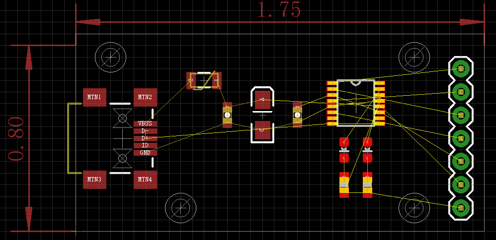
5.把元器件放到一起,尽量紧凑
mini-usb可以放到边界处,Move工具+ctrl点击外框线,使其到网格线上。Note: The USB connector can hang slightly over the edge.

6.整理好后
Take note of a couple things:(画中线看中间的器件是不是符合美学标准)(器件不能太紧,之后还要焊接)
Draw a horizontal line across the middle of the board. You’ll notice I’ve located a lot of the components along the midline. This helps with aesthetics more than anything but also helps with some routing.
Do not attempt to pack everything in right next to each other. You will eventually be soldering these parts to the board and will need some room to get the iron and solder wick in there.

7.最后整理好后

8.布线
Here is a quick breakdown of the key commands we’ll be using:Press F9 to lay a trace
Alt F9 to rip up one
布线让GND 隐藏,之后用敷铜覆盖GND
布线最简单的,然后遇到交叉的就停下来,继续布线其他的
过孔设置I change this to 0.02” (or 0.5mm if you please) and press enter to make Eagle save that size.
布线时shift增加过孔,鼠标中键切换层
(布线网格选择0.05'',所有的器件都选择这个)Note that I keep nearly everything onto the 0.05” grid. This keeps routing and spacing a lot easier. The size (0.05”) is reasonably trivial. The important piece is that all the components and general routing are kept on the same grid.
(有的引脚不在网格上,ALT键可以off grid)While routing, hold the Alt key to jump ‘off grid’. Going off grid is perfectly fine but as a rule of thumb, I try to keep on the grid as much as possible.
9.敷铜Polygon Pours(We need to change the isolate from 0 to 0.012”)
- 敷铜后命名GND
- 敷铜bottom (Now repeat for the bottom polygon pour)
10.DRC检查
- 用SparkFun.dru (软件自带的DRC某系地方有点保守,某些地方bad)
- 之后F8,ratsnest refresh。
The SparkFun DRU file reduces the amount of space between the copper layers and the dimension layer (the border of your board) from 40mil to 10mil.
All these vias should work but they are pretty sloppy. The SparkFun design rules file increases the size of the annular rings around your vias.
Now let’s increase the width of the board outline from 0” to 0.008”.We use the width of the board outline to give us that level of extra safety.
- 外框加粗
- 检查没错之后就可以Adding Labels
- 丝印层‘tPlace’. Anything on tPlace will be printed as silk
- text的大小 We prefer 0.05" or larger so that the text is easier to read
Remember: the PCB fab house has limits to what it can do. We’ve found that anything smaller than 0.04" turns into an unreadable white blob.
(辅助线添加,为了让logo显示在中间)I sometimes have to add some lines on the tDocu layer to show me center point on the board. I draw these in by hand then remove them once I’ve used them to center a logo or text label.
11.健全检查
所有通孔via被焊接mask掩盖,可以任意地方加一个大一点的via看看,DRC规则中在任何小于等于0.02''的孔上solder maskLastly, we add the designer’s name to the PCB and schematic.
12.最后Design Rule Check
(线宽)Normally fab houses don’t want traces thinner than 8mil (0.008”).
13.Gerber Generation
Hit F11 to turn on all the standard layers then click on CAM.
The main gerber files you need to grab:
*.GBL - Bottom copper layer
*.GBO - Bottom overlay (silkscreen)
*.GBS - Bottom soldermask
*.GTL - Top copper layer
*.GTO - Top overlay (silkscreen)
*.GTS - Top soldermask
*.TXT - Drill file (coordinate information)
自己先在gerber viewer上看下,再发给加工厂商gerber viewer
Most fab houses are setup to do:
- Silkscreen one side
- Green soldermask
- White silkscreen
- 1.6mm thick FR4 PCB