{var%20f='http://v.t.sina.com.cn/share/share.php?appkey=1515056452',u=z||d.location,p=['&url=',e(u),'&title=',e(t||d.title),'&source=',e(r),'&sourceUrl=',e(l),'&content=',c||'gb2312','&pic=',e(p||'')].join('');function%20a(){if(!window.open([f,p].join(''),'mb',['toolbar=0,status=0,resizable=1,width=440,height=430,left=',(s.width-440)/2,',top=',(s.height-430)/2].join('')))u.href=[f,p].join('');};if(/Firefox/.test(navigator.userAgent))setTimeout(a,0);else%20a();})(screen,document,encodeURIComponent,'','','https://www.xiaopingtou.cn//data/attach/topic/topicKPo7gB.jpg', '推荐 梦晶 的文章《01-F103RCT6 - PCB绘制之芯片外设》','https://www.xiaopingtou.net/article-91133.html','页面编码gb2312|utf-8默认gb2312'));)
时钟 Clocks and startup
System clock selection is performed on startup, however the internal RC 8 MHz oscillator is
selected as default CPU clock on reset. An external 4-16 MHz clock can be selected, in
which case it is monitored for failure. If failure is detected, the system automatically switches
back to the internal RC oscillator. A software interrupt is generated if enabled. Similarly, full
interrupt management of the PLL clock entry is available when necessary (for example with
failure of an indirectly used external oscillator).
Several prescalers allow the configuration of the AHB frequency, the high speed APB
(APB2) and the low speed APB (APB1) domains. The maximum frequency of the AHB and
the high speed APB domains is 72 MHz. The maximum allowed frequency of the low speed
APB domain is 36 MHz. See Figure 2 for details on the clock tree. 时钟选择是在系统启动前的必要行为 , 在系统复位后,默认启用内部8Mhz时钟 内部晶振频率为8MHZ 外部可接4-16MHZ晶振 APB2 频率可高达72MHZ , APB1频率最高为36MHZ 启动模式 Boot modes At startup, boot pins are used to select one of three boot options:
• Boot from user Flash: you have an option to boot from any of two memory banks. By
default, boot from Flash memory bank 1 is selected. You can choose to boot from Flash
memory bank 2 by setting a bit in the option bytes.
• Boot from system memory
• Boot from embedded SRAM
The boot loader is located in system memory. It is used to reprogram the Flash memory by
using USART1 供电电源约束 Power supply schemes • V DD = 2.0 to 3.6 V: external power supply for I/Os and the internal regulator.
Provided externally through V DD pins.
• V SSA , V DDA = 2.0 to 3.6 V: external analog power supplies for ADC, DAC, Reset
blocks, RCs and PLL (minimum voltage to be applied to VDDA is 2.4 V when the ADC
or DAC is used). V DDA and V SSA must be connected to V DD and V SS , respectively.
• V BAT = 1.8 to 3.6 V: power supply for RTC, external clock 32 kHz oscillator and backup
registers (through power switch) when V DD is not present. VDD : 供STM芯片I/O引脚和内部管理的外部电源 VSSA,VDDA : 供模拟外设(使用ADC ,DAC...必须提供这个引脚电源)的外部电源(模拟外部供电电源) VSSA VDDA必须项链

 VBAT : 实时时钟RTC供电电源 (要不要接?一般RTC是用纽扣电池供电,可以与VDD相连,并且始终精度很高,可以用来计时,日期,闹钟)
定时,日期用
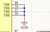
vss : 接地
VBAT : 实时时钟RTC供电电源 (要不要接?一般RTC是用纽扣电池供电,可以与VDD相连,并且始终精度很高,可以用来计时,日期,闹钟)
定时,日期用
vss : 接地
 电源管理 Voltage regulator
The regulator has three operation modes: main (MR), low-power (LPR) and power down.
• MR is used in the nominal regulation mode (Run)
• LPR is used in the Stop modes.
• Power down is used in Standby mode: the regulator output is in high impedance: the
kernel circuitry is powered down, inducing zero consumption (but the contents of the
registers and SRAM are lost)
This regulator is always enabled after reset. It is disabled in Standby mode.
Description STM32F103xC, STM32F103xD, STM32F103xE
18/143 DS5792 Rev 13
2.3.14 Low-power modes
The STM32F103xC, STM32F103xD and STM32F103xE performance line supports three
low-power modes to achieve the best compromise between low-power consumption, short
startup time and available wakeup sources:
• Sleep mode
In Sleep mode, only the CPU is stopped. All peripherals continue to operate and can
wake up the CPU when an interrupt/event occurs.
• Stop mode
Stop mode achieves the lowest power consumption while retaining the content of
SRAM and registers. All clocks in the 1.8 V domain are stopped, the PLL, the HSI RC
and the HSE crystal oscillators are disabled. The voltage regulator can also be put
either in normal or in low-power mode.
The device can be woken up from Stop mode by any of the EXTI line. The EXTI line
source can be one of the 16 external lines, the PVD output, the RTC alarm or the USB
wakeup.
• Standby mode
The Standby mode is used to achieve the lowest power consumption. The internal
voltage regulator is switched off so that the entire 1.8 V domain is powered off. The
PLL, the HSI RC and the HSE crystal oscillators are also switched off. After entering
Standby mode, SRAM and register contents are lost except for registers in the Backup
domain and Standby circuitry.
The device exits Standby mode when an external reset (NRST pin), an IWDG reset, a
rising edge on the WKUP pin, or an RTC alarm occurs.
Note: The RTC, the IWDG, and the corresponding clock sources are not stopped by entering Stop
or Standby mode. 实时时钟 和 备用寄存器 RTC (real-time clock) and backup registers
The real-time clock provides a set of continuously running counters which can be used with
suitable software to provide a clock calendar function, and provides an alarm interrupt and a
DS5792 Rev 13 19/143
STM32F103xC, STM32F103xD, STM32F103xE Description
135
periodic interrupt. It is clocked by a 32.768 kHz external crystal, resonator or oscillator, the
internal low-power RC oscillator or the high-speed external clock divided by 128. The
internal low-speed RC has a typical frequency of 40 kHz. The RTC can be calibrated using
an external 512 Hz output to compensate for any natural quartz deviation. The RTC features
a 32-bit programmable counter for long term measurement using the Compare register to
generate an alarm. A 20-bit prescaler is used for the time base clock and is by default
configured to generate a time base of 1 second from a clock at D2.768 kHz. 实时时钟提供以一个不间断的计数器,可以应用于时钟日历,闹钟 , 定时中断, 定时器和看门狗 Timers and watchdogs
The high-density STM32F103xC/D/E performance line devices include up to two advanced-
定时器和看门狗 Timers and watchdogs
The high-density STM32F103xC/D/E performance line devices include up to two advanced-
control timers, up to four general-purpose timers, two basic timers, two watchdog timers and
a SysTick timer. Independent watchdog
The independent watchdog is based on a 12-bit downcounter and 8-bit prescaler. It is
clocked from an independent 40 kHz internal RC and as it operates independently from the
main clock, it can operate in Stop and Standby modes. It can be used either as a watchdog
to reset the device when a problem occurs, or as a free running timer for application timeout
management. It is hardware or software configurable through the option bytes. The counter
can be frozen in debug mode. 4个多用途计时器,2个基本计时器,2个看门狗,一个滴答定时器 独立看门狗可以在 Stop Standy 模式下工作 总线 I²C bus Up to two I²C bus interfaces can operate in multimaster and slave modes. They can support
standard and fast modes.
They support 7/10-bit addressing mode and 7-bit dual addressing mode (as slave). A
hardware CRC generation/verification is embedded.
They can be served by DMA and they support SMBus 2.0/PMBus. I2C总线,2个ic总线接口,可以用于主从模式,支持标准和快速模式,支持7/10位地址模式,7位模式做位从机使用 串口 Universal synchronous/asynchronous receiver transmitters (USARTs)
 串行接口Serial peripheral interface (SPI)
Up to three SPIs are able to communicate up to 18 Mbits/s in slave and master modes in
串行接口Serial peripheral interface (SPI)
Up to three SPIs are able to communicate up to 18 Mbits/s in slave and master modes in
full-duplex and simplex communication modes. The 3-bit prescaler gives 8 master mode
frequencies and the frame is configurable to 8 bits or 16 bits. The hardware CRC
generation/verification supports basic SD Card/MMC modes.
All SPIs can be served by the DMA controller.、 3个通信速率可达18Mbits/s的主从SPI接口,支持全双工 和 单通道运行, Inter-integrated sound (I 2 S) SDIO Controller area network (CAN) The CAN is compliant with specifications 2.0A and B (active) with a bit rate up to 1 Mbit/s. It
can receive and transmit standard frames with 11-bit identifiers as well as extended frames
with 29-bit identifiers. It has three transmit mailboxes, two receive FIFOs with 3 stages and
14 scalable filter banks.
 Universal serial bus (USB)
GPIOs
采集器ADC
Three 12-bit analog-to-digital converters are embedded into STM32F103xC, STM32F103xD
Universal serial bus (USB)
GPIOs
采集器ADC
Three 12-bit analog-to-digital converters are embedded into STM32F103xC, STM32F103xD
and STM32F103xE performance line devices and each ADC shares up to 21 external
channels, performing conversions in single-shot or scan modes. In scan mode, automatic
conversion is performed on a selected group of analog inputs.
Additional logic functions embedded in the ADC interface allow:
• Simultaneous sample and hold
• Interleaved sample and hold
• Single shunt
DS5792 Rev 13 23/143
STM32F103xC, STM32F103xD, STM32F103xE Description
135
The ADC can be served by the DMA controller.
An analog watchdog feature allows very precise monitoring of the converted voltage of one,
some or all selected channels. An interrupt is generated when the converted voltage is
outside the programmed thresholds.
The events generated by the general-purpose timers (TIMx) and the advanced-control
timers (TIM1 and TIM8) can be internally connected to the ADC start trigger and injection
trigger, respectively, to allow the application to synchronize A/D conversion and timers. 内嵌3个12为模式-数字转换,每个ADC有21外部通道,支持SINGLE-SHOT SCAN模式,SCAN模式会自动转换 可以用DMA传输数据,通常配置定时器TIM 使用

 温度传感器Temperature sensor
下载口 Serial wire JTAG debug port (SWJ-DP)
温度传感器Temperature sensor
下载口 Serial wire JTAG debug port (SWJ-DP)

selected as default CPU clock on reset. An external 4-16 MHz clock can be selected, in
which case it is monitored for failure. If failure is detected, the system automatically switches
back to the internal RC oscillator. A software interrupt is generated if enabled. Similarly, full
interrupt management of the PLL clock entry is available when necessary (for example with
failure of an indirectly used external oscillator).
Several prescalers allow the configuration of the AHB frequency, the high speed APB
(APB2) and the low speed APB (APB1) domains. The maximum frequency of the AHB and
the high speed APB domains is 72 MHz. The maximum allowed frequency of the low speed
APB domain is 36 MHz. See Figure 2 for details on the clock tree. 时钟选择是在系统启动前的必要行为 , 在系统复位后,默认启用内部8Mhz时钟 内部晶振频率为8MHZ 外部可接4-16MHZ晶振 APB2 频率可高达72MHZ , APB1频率最高为36MHZ 启动模式 Boot modes At startup, boot pins are used to select one of three boot options:
• Boot from user Flash: you have an option to boot from any of two memory banks. By
default, boot from Flash memory bank 1 is selected. You can choose to boot from Flash
memory bank 2 by setting a bit in the option bytes.
• Boot from system memory
• Boot from embedded SRAM
The boot loader is located in system memory. It is used to reprogram the Flash memory by
using USART1 供电电源约束 Power supply schemes • V DD = 2.0 to 3.6 V: external power supply for I/Os and the internal regulator.
Provided externally through V DD pins.
• V SSA , V DDA = 2.0 to 3.6 V: external analog power supplies for ADC, DAC, Reset
blocks, RCs and PLL (minimum voltage to be applied to VDDA is 2.4 V when the ADC
or DAC is used). V DDA and V SSA must be connected to V DD and V SS , respectively.
• V BAT = 1.8 to 3.6 V: power supply for RTC, external clock 32 kHz oscillator and backup
registers (through power switch) when V DD is not present. VDD : 供STM芯片I/O引脚和内部管理的外部电源
VSSA,VDDA : 供模拟外设(使用ADC ,DAC...必须提供这个引脚电源)的外部电源(模拟外部供电电源) VSSA VDDA必须项链
VBAT : 实时时钟RTC供电电源 (要不要接?一般RTC是用纽扣电池供电,可以与VDD相连,并且始终精度很高,可以用来计时,日期,闹钟)
定时,日期用
vss : 接地
电源管理 Voltage regulatorThe regulator has three operation modes: main (MR), low-power (LPR) and power down.
• MR is used in the nominal regulation mode (Run)
• LPR is used in the Stop modes.
• Power down is used in Standby mode: the regulator output is in high impedance: the
kernel circuitry is powered down, inducing zero consumption (but the contents of the
registers and SRAM are lost)
This regulator is always enabled after reset. It is disabled in Standby mode.
Description STM32F103xC, STM32F103xD, STM32F103xE
18/143 DS5792 Rev 13
2.3.14 Low-power modes
The STM32F103xC, STM32F103xD and STM32F103xE performance line supports three
low-power modes to achieve the best compromise between low-power consumption, short
startup time and available wakeup sources:
• Sleep mode
In Sleep mode, only the CPU is stopped. All peripherals continue to operate and can
wake up the CPU when an interrupt/event occurs.
• Stop mode
Stop mode achieves the lowest power consumption while retaining the content of
SRAM and registers. All clocks in the 1.8 V domain are stopped, the PLL, the HSI RC
and the HSE crystal oscillators are disabled. The voltage regulator can also be put
either in normal or in low-power mode.
The device can be woken up from Stop mode by any of the EXTI line. The EXTI line
source can be one of the 16 external lines, the PVD output, the RTC alarm or the USB
wakeup.
• Standby mode
The Standby mode is used to achieve the lowest power consumption. The internal
voltage regulator is switched off so that the entire 1.8 V domain is powered off. The
PLL, the HSI RC and the HSE crystal oscillators are also switched off. After entering
Standby mode, SRAM and register contents are lost except for registers in the Backup
domain and Standby circuitry.
The device exits Standby mode when an external reset (NRST pin), an IWDG reset, a
rising edge on the WKUP pin, or an RTC alarm occurs.
Note: The RTC, the IWDG, and the corresponding clock sources are not stopped by entering Stop
or Standby mode. 实时时钟 和 备用寄存器 RTC (real-time clock) and backup registers
The real-time clock provides a set of continuously running counters which can be used with
suitable software to provide a clock calendar function, and provides an alarm interrupt and a
DS5792 Rev 13 19/143
STM32F103xC, STM32F103xD, STM32F103xE Description
135
periodic interrupt. It is clocked by a 32.768 kHz external crystal, resonator or oscillator, the
internal low-power RC oscillator or the high-speed external clock divided by 128. The
internal low-speed RC has a typical frequency of 40 kHz. The RTC can be calibrated using
an external 512 Hz output to compensate for any natural quartz deviation. The RTC features
a 32-bit programmable counter for long term measurement using the Compare register to
generate an alarm. A 20-bit prescaler is used for the time base clock and is by default
configured to generate a time base of 1 second from a clock at D2.768 kHz. 实时时钟提供以一个不间断的计数器,可以应用于时钟日历,闹钟 , 定时中断,
定时器和看门狗 Timers and watchdogs
The high-density STM32F103xC/D/E performance line devices include up to two advanced-control timers, up to four general-purpose timers, two basic timers, two watchdog timers and
a SysTick timer. Independent watchdog
The independent watchdog is based on a 12-bit downcounter and 8-bit prescaler. It is
clocked from an independent 40 kHz internal RC and as it operates independently from the
main clock, it can operate in Stop and Standby modes. It can be used either as a watchdog
to reset the device when a problem occurs, or as a free running timer for application timeout
management. It is hardware or software configurable through the option bytes. The counter
can be frozen in debug mode. 4个多用途计时器,2个基本计时器,2个看门狗,一个滴答定时器 独立看门狗可以在 Stop Standy 模式下工作 总线 I²C bus Up to two I²C bus interfaces can operate in multimaster and slave modes. They can support
standard and fast modes.
They support 7/10-bit addressing mode and 7-bit dual addressing mode (as slave). A
hardware CRC generation/verification is embedded.
They can be served by DMA and they support SMBus 2.0/PMBus. I2C总线,2个ic总线接口,可以用于主从模式,支持标准和快速模式,支持7/10位地址模式,7位模式做位从机使用 串口 Universal synchronous/asynchronous receiver transmitters (USARTs)
串行接口Serial peripheral interface (SPI)
Up to three SPIs are able to communicate up to 18 Mbits/s in slave and master modes infull-duplex and simplex communication modes. The 3-bit prescaler gives 8 master mode
frequencies and the frame is configurable to 8 bits or 16 bits. The hardware CRC
generation/verification supports basic SD Card/MMC modes.
All SPIs can be served by the DMA controller.、 3个通信速率可达18Mbits/s的主从SPI接口,支持全双工 和 单通道运行, Inter-integrated sound (I 2 S) SDIO Controller area network (CAN) The CAN is compliant with specifications 2.0A and B (active) with a bit rate up to 1 Mbit/s. It
can receive and transmit standard frames with 11-bit identifiers as well as extended frames
with 29-bit identifiers. It has three transmit mailboxes, two receive FIFOs with 3 stages and
14 scalable filter banks.
and STM32F103xE performance line devices and each ADC shares up to 21 external
channels, performing conversions in single-shot or scan modes. In scan mode, automatic
conversion is performed on a selected group of analog inputs.
Additional logic functions embedded in the ADC interface allow:
• Simultaneous sample and hold
• Interleaved sample and hold
• Single shunt
DS5792 Rev 13 23/143
STM32F103xC, STM32F103xD, STM32F103xE Description
135
The ADC can be served by the DMA controller.
An analog watchdog feature allows very precise monitoring of the converted voltage of one,
some or all selected channels. An interrupt is generated when the converted voltage is
outside the programmed thresholds.
The events generated by the general-purpose timers (TIMx) and the advanced-control
timers (TIM1 and TIM8) can be internally connected to the ADC start trigger and injection
trigger, respectively, to allow the application to synchronize A/D conversion and timers. 内嵌3个12为模式-数字转换,每个ADC有21外部通道,支持SINGLE-SHOT SCAN模式,SCAN模式会自动转换 可以用DMA传输数据,通常配置定时器TIM 使用
温度传感器Temperature sensor
下载口 Serial wire JTAG debug port (SWJ-DP)