{var%20f='http://v.t.sina.com.cn/share/share.php?appkey=1515056452',u=z||d.location,p=['&url=',e(u),'&title=',e(t||d.title),'&source=',e(r),'&sourceUrl=',e(l),'&content=',c||'gb2312','&pic=',e(p||'')].join('');function%20a(){if(!window.open([f,p].join(''),'mb',['toolbar=0,status=0,resizable=1,width=440,height=430,left=',(s.width-440)/2,',top=',(s.height-430)/2].join('')))u.href=[f,p].join('');};if(/Firefox/.test(navigator.userAgent))setTimeout(a,0);else%20a();})(screen,document,encodeURIComponent,'','','https://www.xiaopingtou.cn//data/attach/topic/topicKPo7gB.jpg', '推荐 不见曦月 的文章《Allegro 常规表贴封装的创建》','https://www.xiaopingtou.net/article-94914.html','页面编码gb2312|utf-8默认gb2312'));)
下面记录了一个普通标贴器件封装的制作过程。1.打开allegro,选择File-New-Package symbol,选择保存路径,然后点击OK。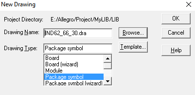 2.设置好设计环境之后,点击Layout-Pin,选择制作好的smd焊盘,
 以制作电感封装为例,下面图片上的X和Y表示在X方向上有1个焊盘,在Y方向上有2个焊盘。
 以电感两个焊盘之间为原点,那么上面焊盘的坐标是(0,3),在command中输入:x 0 3
 点击右键,完成放置。3.在Package Geometry下面添加 SilkScreen_Top ,Assembly_Top ,Place_Bound_Top具体如下:(1)添加 SilkScreen_Top 点击Add-Line,设置如下
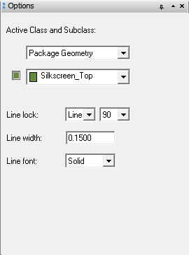
在command中输入起点坐标:x -3.1 3.3,然后向右偏移:ix 6.2,然后向上偏移:iy 6.6,最后输入起始坐标:x -3.1 3.3 (2)添加Assembly_Top将上面绘制的SilkScreen_Top复制一个出来,
然后使用Edit-Change命令转换为Assembly_Top,最后使两者重合即可。 (3)添加Place_Bound_Top在Add-Rectangle
 在器件外框上框选,然后完成即可。4.添加Ref Des中的SilkScreen_Top, Assembly_Top(1)添加SilkScreen_Top选择Add-Text
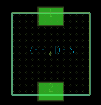 先在command输入:x 0 0,然后输入:ref des 右键完成。(2)添加Assembly_Top步骤和上面一样,只是选择Assembly_Top而已。5.在Component Value下添加SilkScreenAdd-Text,步骤也是和上面一样。

2.设置好设计环境之后,点击Layout-Pin,选择制作好的smd焊盘,以制作电感封装为例,下面图片上的X和Y表示在X方向上有1个焊盘,在Y方向上有2个焊盘。以电感两个焊盘之间为原点,那么上面焊盘的坐标是(0,3),在command中输入:x 0 3 点击右键,完成放置。3.在Package Geometry下面添加 SilkScreen_Top ,Assembly_Top ,Place_Bound_Top具体如下:(1)添加 SilkScreen_Top 点击Add-Line,设置如下在command中输入起点坐标:x -3.1 3.3,然后向右偏移:ix 6.2,然后向上偏移:iy 6.6,最后输入起始坐标:x -3.1 3.3
(2)添加Assembly_Top将上面绘制的SilkScreen_Top复制一个出来,然后使用Edit-Change命令转换为Assembly_Top,最后使两者重合即可。
(3)添加Place_Bound_Top在Add-Rectangle 在器件外框上框选,然后完成即可。4.添加Ref Des中的SilkScreen_Top, Assembly_Top(1)添加SilkScreen_Top选择Add-Text 先在command输入:x 0 0,然后输入:ref des 右键完成。(2)添加Assembly_Top步骤和上面一样,只是选择Assembly_Top而已。5.在Component Value下添加SilkScreenAdd-Text,步骤也是和上面一样。